Series: Digital Design Fundamentals | Article 2
The AND gate that was not there
You wrote assign y = a & b;, ran synthesis, and opened the gate-level netlist
to check something unrelated. There is no AND gate in it. There is a NAND2
feeding an inverter.
Look up both cells in the library databook and it gets stranger. The NAND2 is four transistors. The AND2, which exists, is six, and it is slower. The synthesiser did nothing unusual. It used the AND2 cell, and the AND2 cell is a NAND2 followed by an inverter, because in static CMOS there is no other way to build one.
This article is about why. It covers the two transistors as switches, the pull-down and pull-up networks made from them, why those networks always produce an inverting function, how NAND and NOR fall out of series and parallel arrangements, and why the two are not equally good. It targets anyone who has been handed a standard cell library and wants to know what the numbers in it mean, and anyone learning digital design who wants gates to stop being symbols on a page. It follows on from Digital Design 01, which built the transistors these gates are made of and showed how a gate voltage forms the channel that makes one conduct.
A 1 is a voltage
One thing to settle before any of the schematics make sense: a logic value is not an abstraction sitting on top of the circuit. It is a voltage on a wire.
A digital 1 is the supply voltage, VDD. A digital 0 is ground, 0 V. In these schematics the rail marked VDD and the value 1 are the same thing, and the rail marked GND and the value 0 are the same thing. Saying a gate "outputs a 1" and saying it "connects its output to VDD" describe one event.
VDD is whatever the process runs at, and it has fallen steadily with each node: 5 V in the 1980s, 3.3 V, 1.8 V, and around 0.7 to 0.9 V on a modern logic process. The logic does not care about the number. It cares that there are two rails, that every output can be tied to one of them, and that the receiving gate can tell which.
Real circuits leave margin around both values. Anything above roughly 70 per cent of VDD reads as a 1, anything below roughly 30 per cent reads as a 0, and the band between is the noise margin. A "weak" or "degraded" level later in this article means a voltage that has drifted towards that middle band, where the next gate has to work harder to decide.
Two switches, each good at one thing
The metal-oxide-semiconductor field-effect transistor (MOSFET) has three terminals that matter here: gate, source and drain. Voltage on the gate controls whether current can flow between source and drain. No current flows into the gate itself; it is a capacitor plate over an insulator. That is the whole reason complementary metal-oxide-semiconductor (CMOS) logic can drive thousands of inputs without a power budget for it.
There are two flavours, and they are opposites.
| nMOS | pMOS | |
|---|---|---|
| Conducts when the gate is | high | low |
| Turns on at | gate above source by the threshold voltage | gate below source by the threshold voltage |
| Passes a good | 0 | 1 |
| Passes a poor | 1, stopping a threshold below the supply | 0, stopping a threshold above ground |
| Carrier | electrons | holes |
| Speed for the same width | faster | slower, by roughly two to three times |
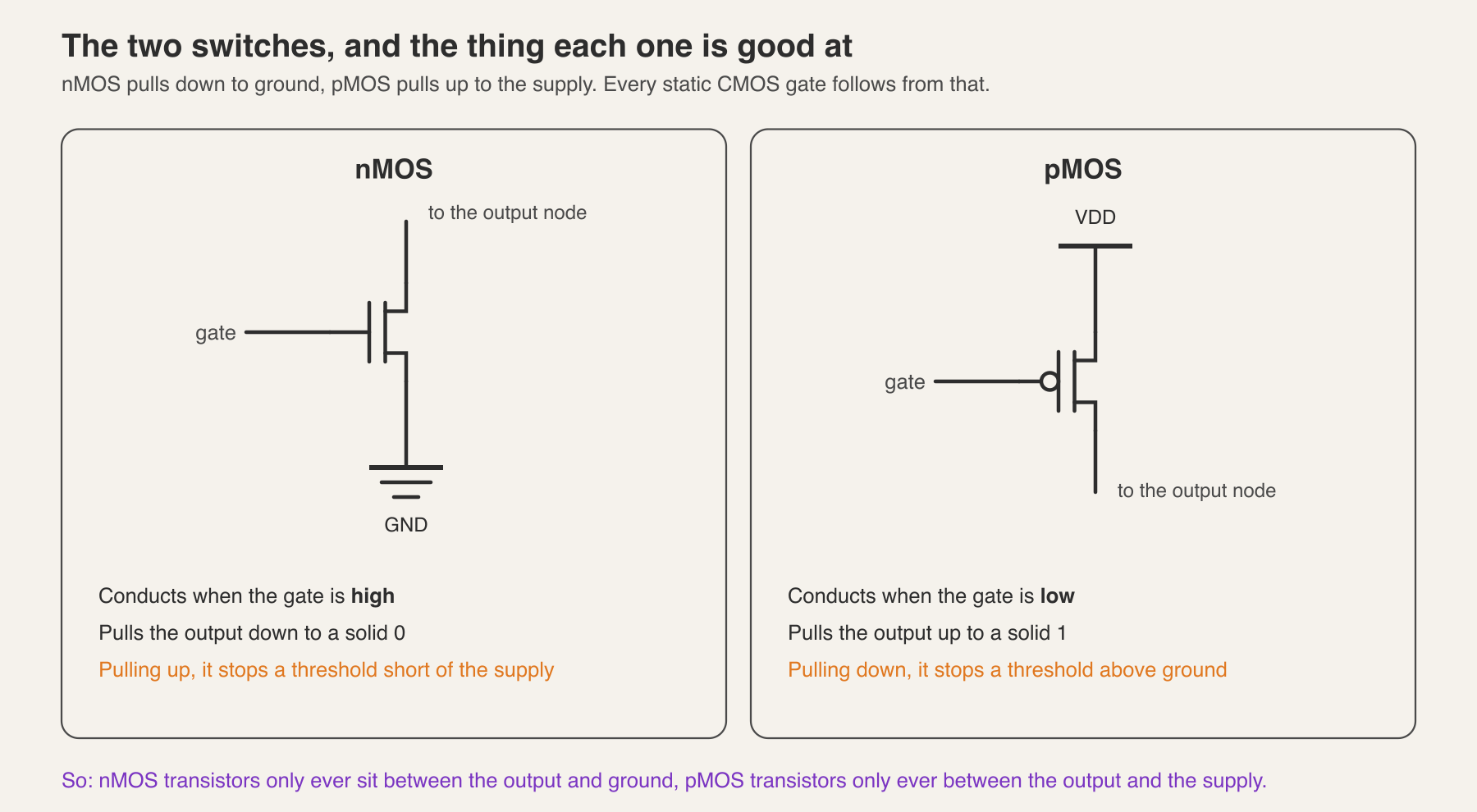
The two rows in the middle of that table are the ones everything else is built on.
Try to pull an output up to the supply through an nMOS. The output rises, and as it rises the gate-to-source voltage falls, because the source is the rising node. When the output gets within one threshold voltage of the gate, the transistor stops conducting. The output sits at roughly the supply minus a threshold: a 1 that is a few hundred millivolts short of VDD, eating into the noise margin above and leaking current in the gate it feeds. The pMOS has the mirror-image problem pulling down to ground.
So the transistors get used the way they are good:
- nMOS transistors connect the output to ground. They form the pull-down network, and their job is producing a solid 0.
- pMOS transistors connect the output to the supply. They form the pull-up network, and their job is producing a solid 1.
Every static CMOS gate is those two networks, sharing the same inputs, sharing the same output node, and arranged so exactly one of them conducts for any combination of inputs. That last property is what "complementary" means, and it has a consequence: when the output is settled, there is no path from supply to ground, so a settled gate draws no current beyond leakage. CMOS burns power when it switches, not when it sits.
The inverter, in full
One nMOS, one pMOS, gates tied together as the input, drains tied together as the output.
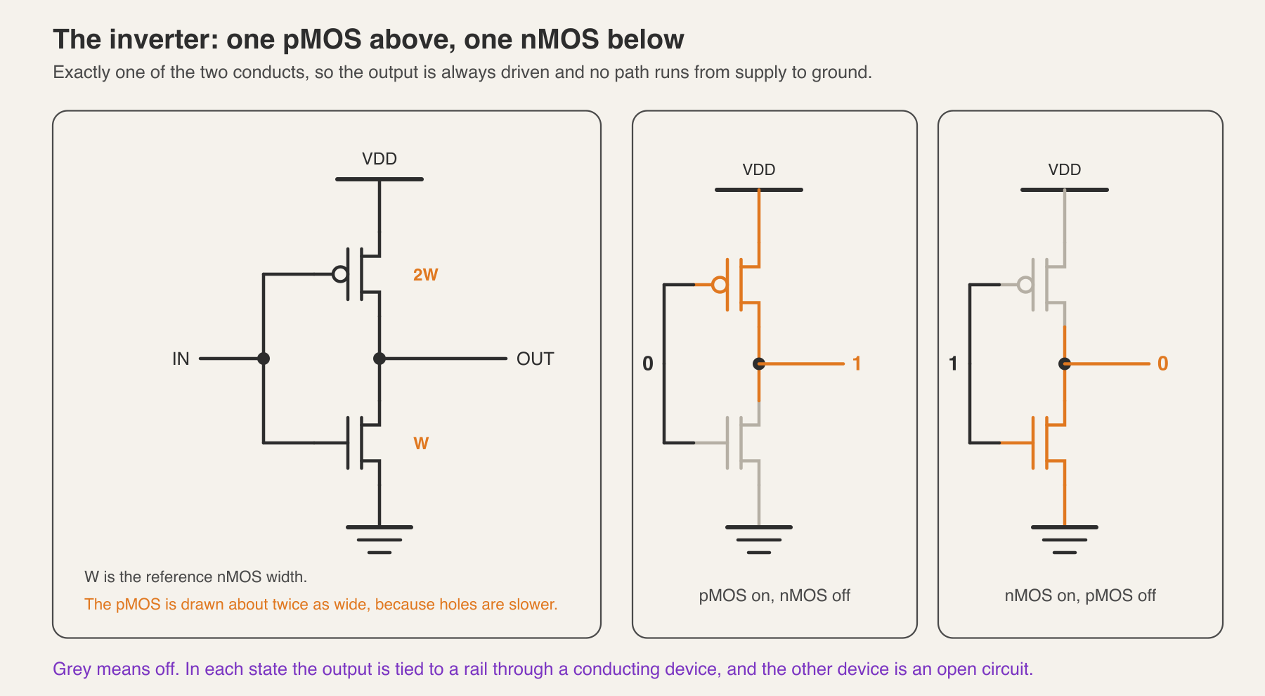
Input low: the pMOS conducts and the nMOS is off, so the output is connected to the supply and pulled to a solid 1. Input high: the nMOS conducts and the pMOS is off, so the output is connected to ground and pulled to a solid 0. Each transistor is used only in the direction it is good at, and in neither state is there a path from supply to ground.
| A | pMOS | nMOS | Output |
|---|---|---|---|
| 0 | on | off | 1 |
| 1 | off | on | 0 |
Two practical points come straight out of the picture.
The pMOS is drawn wider than the nMOS. Holes are slower than electrons by about a factor of two to three, so a pMOS of the same width delivers less current and pulls up more slowly than the nMOS pulls down. Cell libraries compensate by making the pMOS roughly twice the width, which balances rise and fall times at the cost of area and input capacitance. Look at any standard cell layout and the top row of transistors is visibly fatter than the bottom row.
Drive strength is width. An INVX4 is not a different circuit from an INVX1. It is the same two transistors, four times as wide, sourcing four times the current into whatever it drives, and presenting four times the capacitance to whatever drives it. That trade is the entire content of buffer insertion during synthesis: pay input capacitance here to gain drive strength there.
Series and parallel are AND and OR
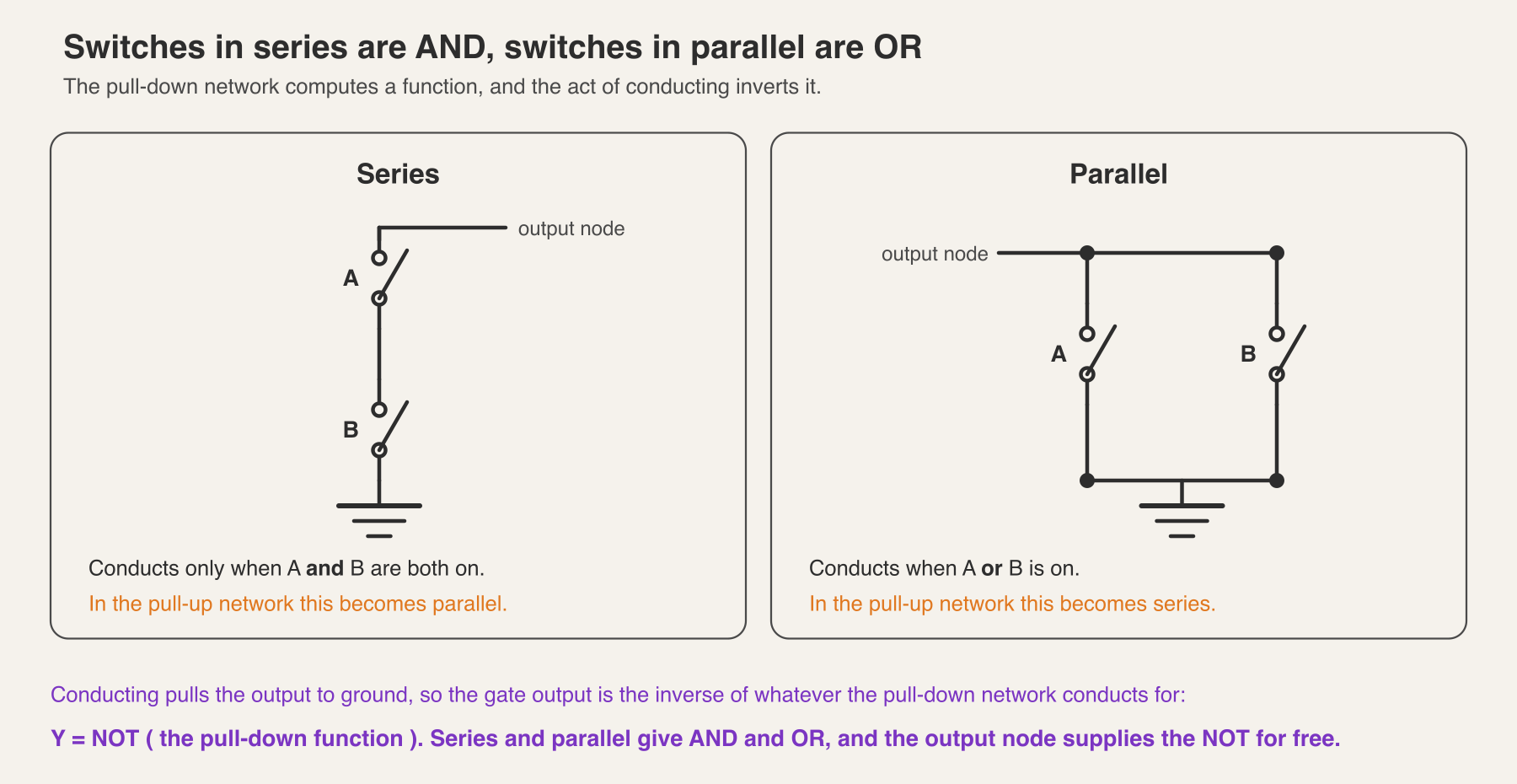
Now build a network out of more than one transistor. Two rules, and they are the whole of it, because a transistor is a switch and switches in series and in parallel behave the way you would expect.
- In series: the path conducts only if both transistors conduct.
- In parallel: the path conducts if either transistor conducts.
Take the pull-down network, made of nMOS, so each transistor conducts when its input is high. Then:
| Pull-down arrangement | Conducts when |
|---|---|
| A in series with B | A AND B |
| A in parallel with B | A OR B |
And here is the step that decides the shape of every gate that follows. The pull-down network pulls the output low. So when the network conducts, the output is 0, and when it does not, the pull-up has it at 1:
output = NOT ( function the pull-down network conducts for )
The pull-down network computes AND and OR of its inputs, and then the output node inverts the answer, because conducting means pulling low. There is no arrangement of nMOS transistors between the output and ground that produces a non-inverting function. Pulling the output down is the only thing such a network can do.
The pull-up network has to be the complement, so that exactly one network conducts at a time. Since pMOS transistors conduct on a low input, the complement comes out as the series-parallel dual: wherever the pull-down has transistors in series, the pull-up has them in parallel, and the other way round. That is De Morgan's theorem drawn as wiring rather than written as algebra.
The recipe for any static CMOS gate is now mechanical:
- Write the function you want as an inverted expression,
y = NOT(f). - Build
fin nMOS between output and ground: AND becomes series, OR becomes parallel. - Build the dual of that network in pMOS between output and supply: series becomes parallel, parallel becomes series.
- Count the transistors. Two per input, always.
NAND2 and NOR2
Apply the recipe to the two simplest cases and the standard cell library appears.
NAND2 is y = NOT(A AND B). AND becomes two nMOS in series to ground. The
dual is two pMOS in parallel to the supply.
NOR2 is y = NOT(A OR B). OR becomes two nMOS in parallel to ground. The
dual is two pMOS in series to the supply.
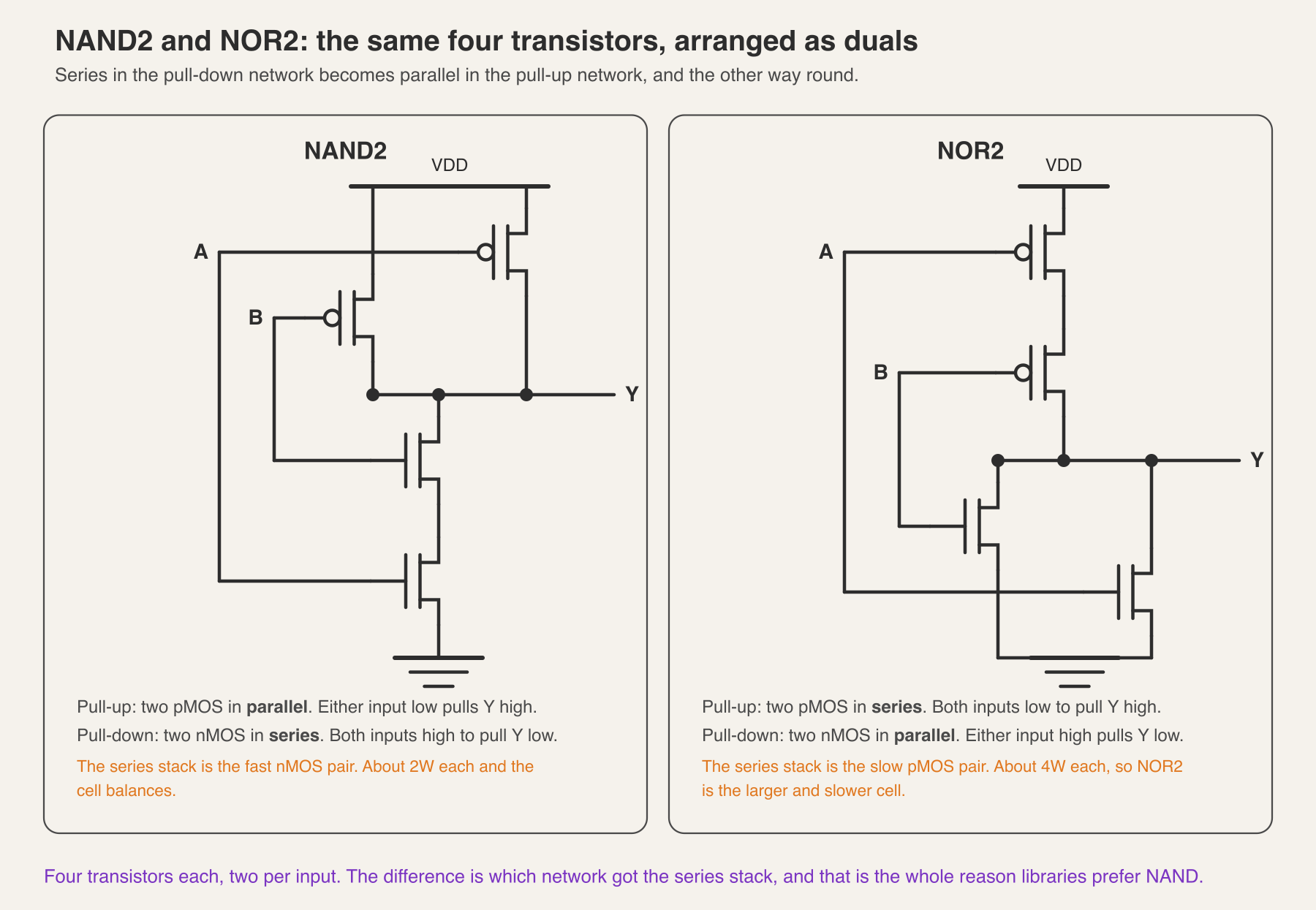
| A | B | NAND2 pull-down | NAND2 out | NOR2 pull-down | NOR2 out |
|---|---|---|---|---|---|
| 0 | 0 | off | 1 | off | 1 |
| 0 | 1 | off | 1 | on | 0 |
| 1 | 0 | off | 1 | on | 0 |
| 1 | 1 | on | 0 | on | 0 |
Four transistors each, symmetric on paper. They are not symmetric in silicon.
In NAND2 the slow transistors, the pMOS pair, are in parallel, so either one alone can pull the output up, and each can stay near the minimum practical width that balances the gate. The nMOS pair is in series, so two channel resistances add on the pull-down, and each nMOS is roughly doubled in width to compensate. Electrons are cheap to widen.
In NOR2 it is the other way round, and the arrangement falls the wrong way. The pMOS pair is in series, so two already-slow devices add their resistances, and getting a rise time to match the fall time means widening each of them by something like four times the nMOS width. That is a bigger cell, more input capacitance presented to whatever drives it, and a worse delay for the same logical work.
This is why libraries and synthesis are NAND-heavy. Given a choice between two logically equivalent structures, the one built from NAND2 and inverters is usually smaller and faster than the one built from NOR2. It is also why a four-input NOR is rare, and a four-input NAND uncommon: stacking four pMOS in series produces a cell whose pull-up is several times slower than its pull-down, and stacking any four devices runs into the body effect, where transistors part-way up a stack see a raised source voltage, an effectively higher threshold, and less current than the one at the bottom. Practical libraries stop at three or four inputs and let synthesis build trees from there.
Where the AND gate's extra transistors went
Back to the netlist that started this. The recipe produces y = NOT(f), always.
The output node is pulled low by a conducting network, and there is no way to
arrange switches so that conducting pulls it high while still using nMOS below
and pMOS above. A single-stage static CMOS gate is inverting by construction.
So AND2 is NAND2 plus an inverter: 4 + 2 = 6 transistors, two stages of delay rather than one. OR2 is NOR2 plus an inverter, and inherits the NOR2 pull-up problem as well. A buffer is two inverters, for the same reason. Nothing in the library is non-inverting for free.
NAND and NOR are not "universal gates" because of a tidy algebraic fact about being able to express everything with them. They are the gates the libraries are built from because a pull-down network and its dual produce them naturally, and AND and OR are the compound cells, sold at a two-transistor and one-stage premium. The Boolean operators you write in a hardware description language are the abstraction. The inverting cells are the hardware.
Two habits follow from it.
Push the inversions around instead of paying for them. De Morgan says a NAND with inverted inputs is an OR, and a NOR with inverted inputs is an AND. An inverter that cancels another inverter is free once the netlist is optimised, and a bubble that moves to a place where something else already inverts costs nothing at all. Synthesis does this automatically, which is why the netlist so rarely resembles the RTL structurally.
Compound functions can stay in one stage. The recipe never said the network
had to be two transistors. y = NOT((A AND B) OR C) is an and-or-invert
gate, AOI21: two nMOS in series for the AND, that pair in parallel with a third
for the OR, and the dual above it. Six transistors, one stage of delay, and it
does the work of an AND2 feeding a NOR2, which would have cost ten
transistors and three stages.
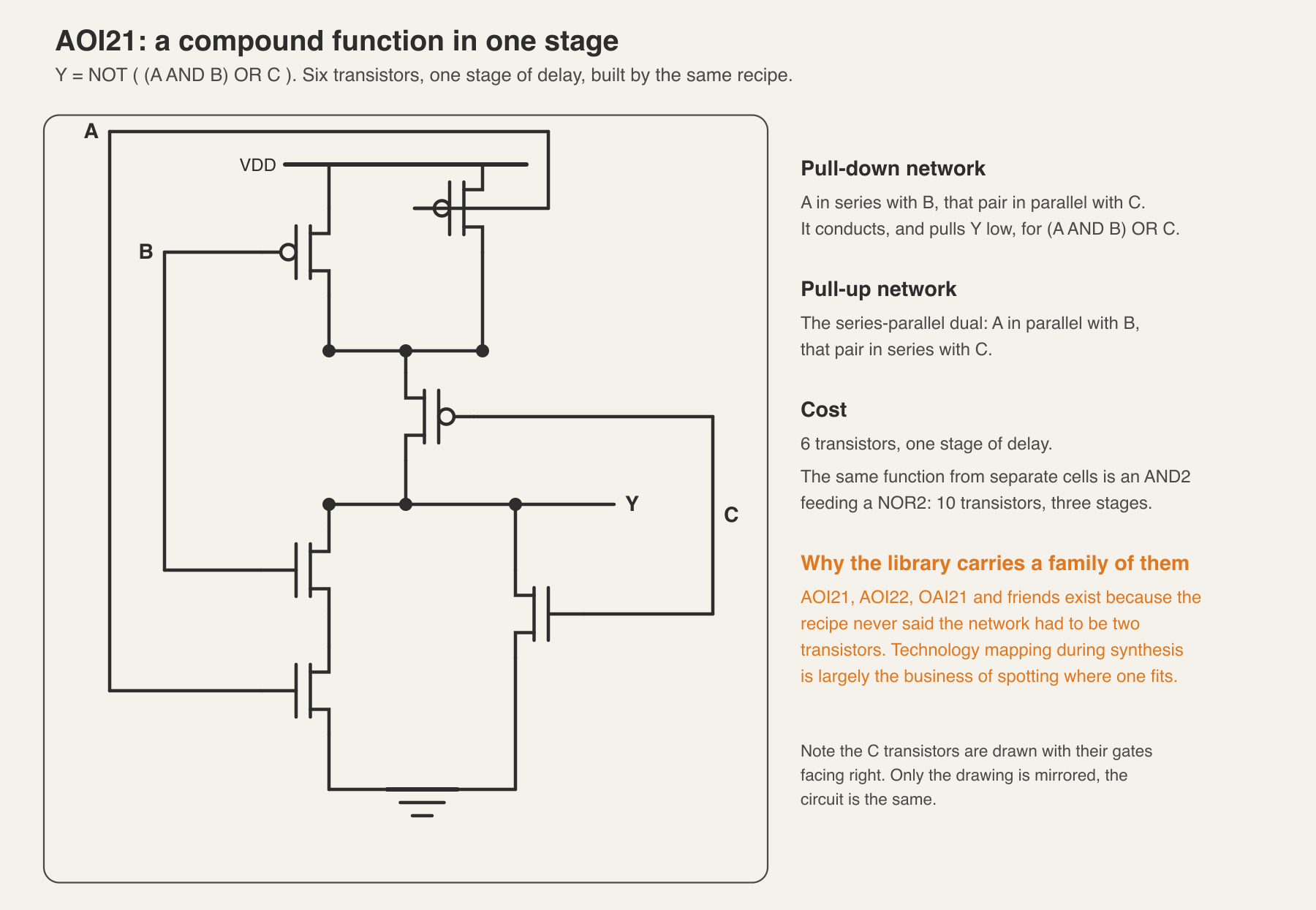
Libraries carry a whole family of these: AOI21, AOI22, OAI21, OAI221 and more. Technology mapping during synthesis is largely the business of spotting where one of them fits, and it is a large part of why hand-instantiated gate-level logic so seldom beats the tool.
The two things static CMOS is bad at
Two functions resist the recipe, and both are common enough that libraries solve them another way.
The multiplexer. Selecting between two inputs as a static CMOS gate is an AOI22 at eight transistors, one inverter to make the complement of the select and another to restore the polarity: twelve transistors for a function that only has to connect one of two wires to an output. The alternative is a transmission gate: an nMOS and a pMOS in parallel, driven by complementary select signals, acting as a switch that passes a full-strength signal in either direction. The nMOS covers the low end, the pMOS covers the high end, and between them the weak-1 and weak-0 problems cancel. Two transmission gates and an inverter make a clean two-way multiplexer.
Exclusive-OR. In pure static CMOS, XOR needs both inputs and their complements and lands at ten to twelve transistors. Built from transmission gates it comes down to six or eight. Since XOR is the core of every adder and every parity tree, that saving justifies the library carrying special cells for it, and it is why an adder's transistor count never quite matches the figure the gate count suggests.
The catch with transmission gates is that they pass signals rather than drive them. A chain of them accumulates resistance quadratically and has no gain to restore a degraded edge, so a buffer has to appear every couple of stages. Transmission-gate logic is a local optimisation inside a cell, not a style for building a whole design.
Reading a cell library like a circuit
The next time a databook is open, the numbers have physical meanings.
- Transistor count, or the area column standing in for it: two per input for a simple gate, plus two for every inversion the function needs at the output. A six-transistor two-input cell is a compound gate with an inverter on it.
- Input capacitance differs per pin on the same cell. In a NAND2 the input nearest the output in the nMOS stack switches faster than the one nearest ground, which is why the timing model gives per-pin arcs and why synthesis cares which signal lands on which pin.
- A NOR2 that is larger than the NAND2 of the same drive strength is the series pMOS stack, sized up. If a design is NOR-heavy, that is showing up in both area and timing.
- Drive strength suffixes are transistor width. More output current, more input capacitance, no change to the logic.
- Rise and fall times that differ mean the pull-up and pull-down networks are not balanced, either by design or because the cell was optimised for area.
Every one of those numbers is a pull-up network and a pull-down network, drawn as polygons on the masks from the previous article, and the standard cell layout is where the two articles meet: the p-type row along the top under a supply rail, the n-type row along the bottom over a ground rail, polysilicon stripes crossing both to form the gates, and metal 1 stitching the drains together into the output.
From here the series splits, and the two branches do not depend on each other.
One branch wires these cells into a loop and asks what happens when the loop holds neither a 0 nor a 1: metastability, and the unreproducible bugs that follow when two gates read the same undecided wire and disagree.
The other branch keeps the cells combinational and starts combining them: Boolean algebra as a tool for restructuring logic before it ever reaches a transistor.
Previous: Digital Design 01: Mask sets, and how a transistor gets built Next: Digital Design 03: Metastability